En caso de que alguien quiera hacer uso de la tecnología del SVP, aquí tenéis información.
Nombre a la venta: Samsung SSP1601
Descripción: DSP de puto fijo a 16 bits.
Encapsulado: TQFP-68
Voltaje de entrada: 5V.
PINOUT:
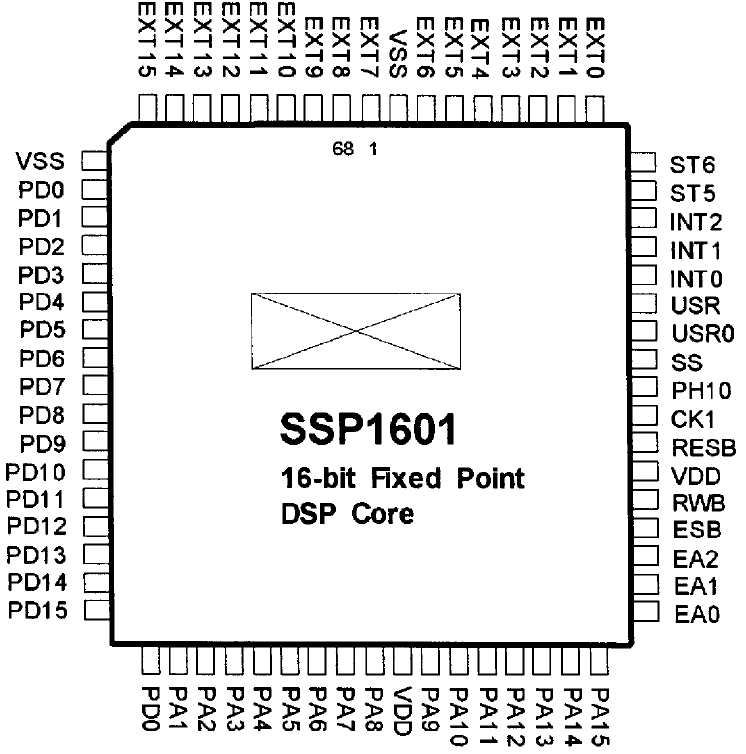 DESCRIPCIÓN DE LOS PINES:
CK1: señal de reloj (CLK). Conectar a CLK (cart slot) o usar oscilador propio.
PH10B: salida de reloj interna.
RESB: paso asíncrono, efectivo cuando CK1 está activo.
SS: paso asíncrono único, efectivo cuando se produce un ciclo de CK1.
INT0-2: petición de interruptor.
PA0-PA15: bus de dirección.
PD0-PD15: bus de datos.
EXT0-EXT15: bus de expansión.
EA0-EA2: bus externo de registro.
ESB: strobe de datos externo (¿conectar a strobe de 68k?).
R/W: interruptor para definir si se escribe o se lee del bus de expansión.
USR0-USR1: entrada de datos personalizada.
VDD: +5V.
VSS: ground.
ST5-ST6: salida de datos personalizada.
CARACTERÍSTICAS FÍSICAS:
Temperatura de almacenado: de -65 ºC a 110 ºC.
Temperatura de soldado: menos de 300 ºC.
Gasto energético: 40 miliamperios (reloj (CK1) funcionando a 25 MHz).
HERRAMIENTAS DE DESAROLLO:
Contactar con Samsung Electronics para conseguirlas.
Ensamblador y documentación: MASM1601.
Enlazador: LNK1601.
Separador de ROM's: RSP1601.
Emulador / simulador: SIM1601.
Todas las herramientas son para MS-DOS. Necesitarás un sistema operativo anterior a Windows Milenium Edition, Dos-Box, MS-DOS 4.XX ó similar.
DESCRIPCIÓN OFICIAL:
Samsung Electronics DSP 1601 Datasheet escribió:Samsung is a pioneer in the DSP core approach, which is a high performing and flexible family of DSP core based ASDSP (Application Specifics Digital Signal Processor). The DSP core architecture and instruction set are designed simplicity and flexibility. The DSP core contains only the most essential DSP function blocks. Because all internal buses are accessible externally. The ASDSP is an application specifics integrated sircuit that incorporates a programmable digital signal processor core. The ASDSP approach allows the system designer to integrate a programmable dsp core, interface logic, peripheral, extra memory into a single integrated circuit. Typically, the custom circuitry on a ASDSP is implemented either in standard cell or gate array. All methods used samsung process by 0.8um double metal CMOS technology.
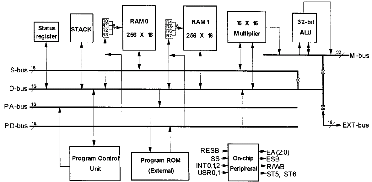
The SSP1601 uses 0.8um CMOS technology (CSP4H) and can perform up to 25 MHz at 5V. The SSP1601 DSP cores have the following on-chip functions:
two independent high-speed RAM banks
a 16x16 multiply unit
an 32-bit ALU
RAM address pointers
a status register
a program control unit
an external bus control unit
The DSP core can address up to 64K-word of external ROM over an external data bus. The actual size of the external ROM area used depends upon the requirements of the individual application. The SSP1601 has five 16-bit buses and one 32-bit bus:
program address (PA) bus
program data (PD) bus
multiplier (M) bus
external (EXT) bus
subsidiary (S) bus
data (D) bus.
MPYA instructions (add, load, multiply, and modify RAM address pointer) are executed efficiently within one machine cycle. The condition flags in the status register (ST) are set or cleared by the corresponding ALU operations. Values for the status register control bits are loaded by application software or through the I/O pins USR0, USR1, ST5 and ST6.
The system stack has six hardware levels and operates using Push and Pop operations. The pins EA[2:0], ESB and R/WB are used to control the EXT bus, and the RESB, INT0, INT1, INT2 and SS pins are used to control system functions.
LISTA DE CARACTERÍSTICAS OFICIAL: Samsung Electronics DSP 1601 Datasheet escribió:16-bit fixed point arithmetic
ACC + A x B -> ACC; MAC operation in 40ns using pipelined multiplier
16x16-bit pipelined multiply with 32-bit output
32-bit ALU operation
512-word data RAM; RAM0, RAM1
Eight 8-bit RAM point registers:
R0 ~ R3 for RAM0
R4 ~ R7 for RAM1
RAM pointer registers for easy circular buffer operation
Simple instruction set
User defined I/Os
Up to 64K word Program Memory which can be readable and writable
SSP1601 EVA Chip (additional) has two 256-word SRAM for each RAM bank
25 MIPS @ 5.0 Volt
68-pin PLCC (evaluation version
0.8um double metal CMOS (CSP4H)
Excepted core size (except PAD, Data RAM): 3600um x 2400um
DIAGRAMA DE FLUJO:
Espero que lo disfrutéis.
Saludos, andoba.
